Gallium Nitride GaN Device Mainstream – 600V GaN D-mode HEMT Introduction
GaN,Latest Articles
October 28, 2021
AFor the current
gallium nitride GaN
, the proper nouns and abbreviations are as follows, which helps us understand the specifications and uses of gallium nitride GaN. This article is an introduction to gallium nitride GaN, and collects related articles from the Internet to help further understand the use of gallium nitride GaN.
HEMT : High Electron Mobility Transistors
MIS-HEMT : Metal-Insulator-Semiconductor -High Electron Mobility Transistors
E-mode GaN : Enhancement-mode GaN
D-mode GaN : Depletion-mode GaN
Gross die: 一片wafer有多少顆產品。一般而言,目前GaN wafer 是6吋晶片。
2DEG: two dimensional  electron  gas(二維電子氣通道)
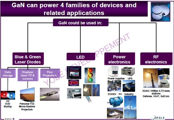
We start from the gallium nitride GaN market and applications, including gallium nitride GaN process, gallium nitride GaN structure and related differences. The future gallium nitride GaN will be gallium nitride GaN on SiC and the structure is vertical. In consideration of cost and process capability, the current mainstream market is the horizontal structure of GaN on Si, and 6-inch chips are the main products.
Table of contents:
Gallium Nitride GaN Markets, Applications, Especially in Power Electronics:


Gallium Nitride GaN Construction:

Gallium nitride GaN process:

Equivalent circuits of E-mode and D-mode:

E-mode GaN D-mode GaN(Cascode)
The main reason is that the Vt of D-mode GaN is negative, and an additional Mos is needed to form a normal Off. In E-mode itself, it is already normal to turn Vt positive by using manufacturing processes and other methods.
Differences between HEMS and MIS-HEMT:

Future construction of gallium nitride GaN:

The future structure of gallium nitride GaN will also change from the current horizontal direction to the vertical direction.
Application of gallium nitride GaN power devices in the fast charging market:

Application fields of gallium nitride GaN and silicon carbide SiC:
